Diode
1
- Semi-conductors
1.1 - What is semiconductor?
Quality semiconductor materials to produce all kinds of semiconductors such as Diode, Transistor, IC, but we have seen in the electronic equipment on this. Semiconductors are substances that have characteristics intermediate between electrical conductors and insulators, in terms of chemistry, the semiconductor is substances have four electrons in the outermost layers of atoms. That is the nature
Germanium (Ge) and Silicium (Si) From the initial semiconductor (pure) one must create two types of transistors are N type semiconductor and semiconductor type P, then assembling pieces of N and P type semiconductor obtained the diode or transistor. Si and Ge has four valence, ie the outer layer is 4. Electronics, in the possible pure Si atoms (Ge) linked together by covalent links as shown below.

* When we mix a small amount of substances such as chemotherapy 5 Phospho (P) in nature Si transistor is a P atom linked to four Si atoms in contact plus the chemotherapy, only 4 phosphorus atoms involved electronic link and the remaining one electron and become free electrons => Semiconductor at become redundant electronics (electrically negative) and are called semiconductors N (Negative: negative).


2 - Diode (diodes) Semiconductors
2.1 - Adjoining P - N and the composition of the semiconductor diode.
There are two semiconductors are P and N, if the coupling of two semiconductors in an adjacent P - N It is a diode, P-N junction is characterized by : At the contact surface, the excess electron diffusion in semiconductors N to the semiconductor region P to fill the holes => form a Ion electrically neutral => domain layer constitutes Ion insulation between two semiconductors.


3.1 - Zener Diode
* Components:
Diode Zener diode has a structure similar but usually have two layers of semiconductor P - N coupled together, Zener diode is used in the polarization mode contrast, when polarized upon as diode zener diode normally distributed but inverse zener diode will reduce the voltage to a fixed value recorded on the diode.


3.3 - emitting diode (Diode Emiting Light: LED)
Diode developed planar light emitting diode being polarized upon, the voltage LED work of about 1.7 => 2.2 V line via Led range from 5mA to 20mA LEDs are used to make light sources, flash design, power status. etc. ...


1.1 - What is semiconductor?
Quality semiconductor materials to produce all kinds of semiconductors such as Diode, Transistor, IC, but we have seen in the electronic equipment on this. Semiconductors are substances that have characteristics intermediate between electrical conductors and insulators, in terms of chemistry, the semiconductor is substances have four electrons in the outermost layers of atoms. That is the nature
Germanium (Ge) and Silicium (Si) From the initial semiconductor (pure) one must create two types of transistors are N type semiconductor and semiconductor type P, then assembling pieces of N and P type semiconductor obtained the diode or transistor. Si and Ge has four valence, ie the outer layer is 4. Electronics, in the possible pure Si atoms (Ge) linked together by covalent links as shown below.
Pure semiconductors.
1.2 - N type
semiconductor * When we mix a small amount of substances such as chemotherapy 5 Phospho (P) in nature Si transistor is a P atom linked to four Si atoms in contact plus the chemotherapy, only 4 phosphorus atoms involved electronic link and the remaining one electron and become free electrons => Semiconductor at become redundant electronics (electrically negative) and are called semiconductors N (Negative: negative).
N semiconductors
1
.3 - P type semiconductor
In contrast, when we added a small amount of a third
chemotherapy as Indium (In) on Si is a
semiconductor material Indium atoms will link with
four Si atoms linked by covalent and a missing link e => into holes (positively charged) and the called semiconductors
P.
Semiconductor P
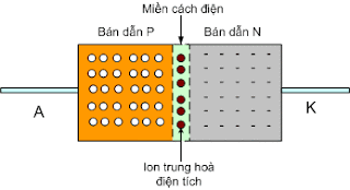
2 - Diode (diodes) Semiconductors
2.1 - Adjoining P - N and the composition of the semiconductor diode.
There are two semiconductors are P and N, if the coupling of two semiconductors in an adjacent P - N It is a diode, P-N junction is characterized by : At the contact surface, the excess electron diffusion in semiconductors N to the semiconductor region P to fill the holes => form a Ion electrically neutral => domain layer constitutes Ion insulation between two semiconductors.

Termites exposed P - N =>
Anatomy of the diode.
* The
contact form on the relationship P - N and also the structure of a semiconductor
diode.
Symbols and shape of a
semiconductor diode.
2.2
- Polarization upon to diode.
Have a positive voltage (+) to the anode (P semiconductor regions) and negative voltage (-)
in Katot (semiconductor region N), then the interaction effect of power pressure, shrinking domain insulation, keeping the voltage difference between the two poles meet 0.6 V (with Si diode type) or 0.2 V (with diode type Ge) is the domain analysis insulation reduced to zero => Diode start conducting. If continue to increase the voltage across the diode current increased but the difference
voltage difference between the two poles of the diode does not increase (remained the same at 0.6 V)
Diode (Si) polarization upon -
When Dode lead
agreement, the reduce voltage at 0.6 V
agreement, the reduce voltage at 0.6 V
Line voltage characteristic of
the agreement through the diode
* Conclusion: The
diode (type Si) agreement is
polarized, if the voltage polarity upon <0.6 V is not
currents through the diode, if the polarization voltage = 0.6 V, the agreement reached with the line passing through Diode current through the diode and then increased rapidly but still keep pressure drop agree at 0.6 V value.
currents through the diode, if the polarization voltage = 0.6 V, the agreement reached with the line passing through Diode current through the diode and then increased rapidly but still keep pressure drop agree at 0.6 V value.
2.3
- Diode for reverse polarity.
When the polarity is opposite to the diode power (+) in Katot
(sold Guide N), source
(-) to anode (P transistors), the interaction of the voltage contrast, the wider domain insulator and prevents current
through contiguous
relationship, diode can withstand very large reverse voltage about
1000V, the new diode is punctured.
Diode only fires
when the voltage of opposite polarity increases> = 1000V
2.4
- Methods of measurement Diode test
Measuring Diode test
Set the clock in
the scale x 1Ω, which put two sticks on either end Diode, if: Upon measuring the anode rod black, red stick on
Katot => kim up, reversing the needle does not measure up is => Diode good If measured on both
clockwise = 0Ω => a diode has been short. If the needle is not
measured positively up => is diode breaks. In measurements on the diode D1 well,
diode D2 and D3 has been short-cuts If the
measure to scale back on Diode 1KΩ metal is still a little diode
detectors.
2.5
- Application of Semiconductor Diode.
* Do one-dimensional conductive properties
should Diode commonly
used in the rectifier AC into a
way, the detector circuit, the circuit to reduce voltage polarity transistor operation the. the rectifier diode can be integrated into a diode bridge of the form.
way, the detector circuit, the circuit to reduce voltage polarity transistor operation the. the rectifier diode can be integrated into a diode bridge of the form.
The diode bridge
rectifier ac.
3
- Types of Diode 3.1 - Zener Diode
* Components:
Diode Zener diode has a structure similar but usually have two layers of semiconductor P - N coupled together, Zener diode is used in the polarization mode contrast, when polarized upon as diode zener diode normally distributed but inverse zener diode will reduce the voltage to a fixed value recorded on the diode.
Shape Zener diode (DZ)
Symbols and applications of
zener diode in the circuit.
The above diagram illustrates the
application of DZ, U1 is the power source voltage change, dz is the diode
voltage, R1 is to limit the line. We see that the source U1> dz dz shall always fixed on whether
U1 source changes. As U1 source changes, the change back through DZ, DZ
efflux through a limiting value of about 30mA. Usually people use source
U1> 1.5 => 2 DZ was more
fitting term and the R1 so that the most backward through the DZ<30mA.
If U1
<U1 DZ when pressure changes and changes in the DZ
If U1> DZ change when U1 => constant pressure on the DZ.
If U1> DZ change when U1 => constant pressure on the DZ.
3.2 - Optical Diode
Thu. (Photo Diode)
Diode optical receiver operating in reverse polarity mode, with a piece of shell diode glass to the light on the relationship P - N, the current through the diode reverse proportional to light intensity in the diode.
Diode optical receiver operating in reverse polarity mode, with a piece of shell diode glass to the light on the relationship P - N, the current through the diode reverse proportional to light intensity in the diode.
Symbols of Photo Diode
Illustrate the operation of Photo
Diode
3.3 - emitting diode (Diode Emiting Light: LED)
Diode developed planar light emitting diode being polarized upon, the voltage LED work of about 1.7 => 2.2 V line via Led range from 5mA to 20mA LEDs are used to make light sources, flash design, power status. etc. ...

Emitting diodes LED
3.4
- Diode varicap (variable capacity diode)
Content is variable Diode Diode capacitance as a capacitor, and capacitance changes when we change the voltage on the diode reverse order.
Content is variable Diode Diode capacitance as a capacitor, and capacitance changes when we change the voltage on the diode reverse order.
Capacity variable diode un of varicap (V D)
in the resonant circuit
In the philosophy of regulation when
applying VR, the voltage put to
the diode reverse varicap changes, changes the capacitance of the diode
=> Changes the resonance frequency of the circuit.Variable capacity diode used in the color
of television channels, in the circuit to adjust the resonant frequency by
voltage.
3.5 - Diode pulse
In the power pulse at the output of the pulse transformer, we must use the Diode pulse for rectifiers. pulse diode diode is working at high frequencies of a few tens of KHz, conventional diode rectifier can not replace the positiondiode pulse, whereas pulse diode can replace position regular diode, diode pulses with a higher cost diode is often many times. Characteristics, the diode pulse shape is not any different with Diode often, but usually the next pulse Diode dashed or marked marked by two rounds
In the power pulse at the output of the pulse transformer, we must use the Diode pulse for rectifiers. pulse diode diode is working at high frequencies of a few tens of KHz, conventional diode rectifier can not replace the positiondiode pulse, whereas pulse diode can replace position regular diode, diode pulses with a higher cost diode is often many times. Characteristics, the diode pulse shape is not any different with Diode often, but usually the next pulse Diode dashed or marked marked by two rounds
The symbol of the diode pulse
3.6 - Diode
detector.
Diode is a type of glass and small notebooks called diode
contacts for contact
surface between the semiconductor P - N at a point to avoid power parasitic capacity, diode detector commonly used in high
frequency circuits used for signal detection.
3.7 - Diode
rectifier.
As the diode rectifier to the surface for the 50Hz AC
power rectifier , Usually have three types of diode is
1A, 2A and 5A.
5A diode rectifier